  |
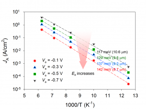
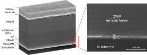
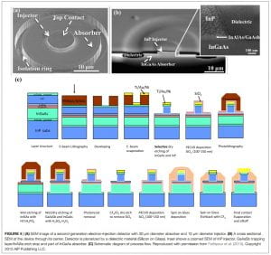
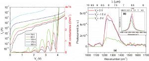
InGaAs/InP quantum well infrared photodetector integrated on Si substrate by Mo/Au metal-assisted wafer bondingMin-Su Park, Mohsen Rezaei, Iman Nia, Robert Brown, Simone Bianconi, Chee Leong Tan, and Hooman Mohseni Optical Materials Express Vol. 8, Issue 2, pp. 413-419 (2018) |
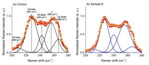 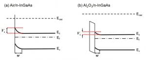 |
Surface passivation and aging of InGaAs/InP heterojunction phototransistorsMin-Su Park, Mohsen Razaei, Katie Barnhart, Chee Leong Tan, Hooman Mohseni Journal of Applied Physics 121, 233105 (2017) |
 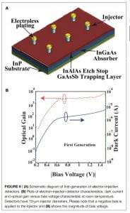 |
Advances on Sensitive Electron-Injection Based Cameras for Low-Flux, Short-Wave Infrared ApplicationsVala Fathipour, Alireza Bonakdar, Hooman Mohseni Front. Mater. 3, (2016). |
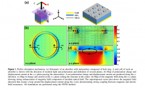 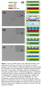 |
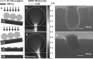
High-throughput realization of an infrared selective absorber/emitter by DUV microsphere projection lithographyAlireza Bonakdar, Mohsen Rezaei, Eric Dexheimer, Hooman Mohseni Nanotechnology, 3(27), (2015). |
 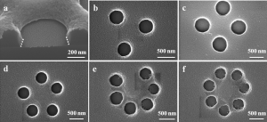 |
Novel high-throughput and maskless photolithography to fabricate plasmonic molecules,A. Bonakdar, S. J. Jang and H. Mohseni Journal of Vacuum Science & Technology B (2014) |
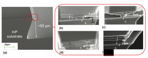 |
Precise formation of dovetail structures for InP-based devicesI. H. Nia and H. Mohseni ECS Solid State Letters (2013) |
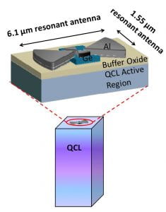 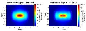 |
Antenna integrated quantum cascade laser switchable via telecommunications wavelength probe beamJ. Kohoutek, A. Bonakdar, R. Gelfand, D. Dey, I. Hassani, V. Fathipour, O. G. Memis, and H. Mohseni SPIE Optics+Photonics (2012) |
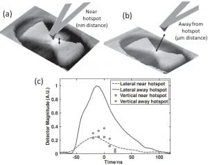 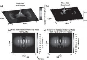 |
Mechanical frequency and amplitude modulation of quantum cascade laser integrated with plasmonic nanoantennaJ. Kohoutek*, D. Dey*, A. Bonakdar, R. Gelfand, V. Fathipour, O. G. Memis, and H. Mohseni Small, (2012) |
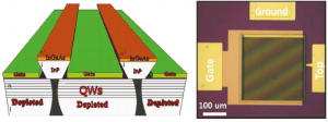  |
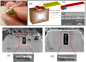
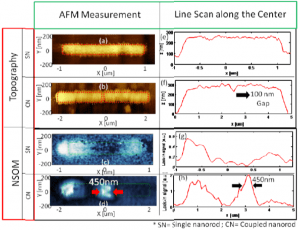
Interlevel Cascade Transition in Electrically Confined Quantum Wire ArraysW. Wu, I. Hassani, and H. Mohseni ACS Nano 5 (9), 7488-7493, (2011) |
  |
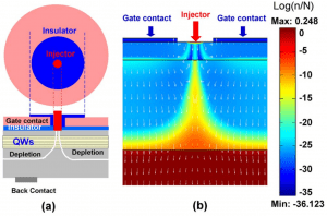
A new generation of mid-infrared sensors based on quantum cascade laserD. Dey, J. Kohoutek, R. M. Gelfand, A. Bonakder, and H. Mohseni Proc. SPIE 8034, 803404 (2011) |
 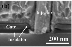 |
Modeling and fabrication of electrically tunable quantum dot intersubband devicesW. Wu, D. Dey, O. G. Memis, and H. Mohseni, Applied Physics Letters (2009) |
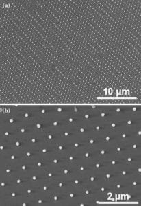 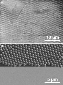 |
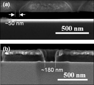
Fabrication of Large Area Periodic Nanostructures Using Nanosphere PhotolithographyW. Wu, D. Dey, O. G. Memis, A. Katsnelson, and H. Mohseni Nanoscale Research Letters (2008) |
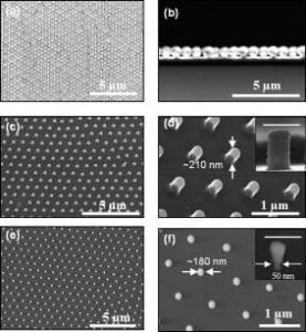  |
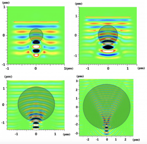
Large areas of periodic nano-holes perforated in multi-stacked films produced by lift-offW. Wu, D. Dey, A. Katsnelson, O. G. Memis, and H. Mohseni Journal of Vacuum Science and Technology B (2008) |
 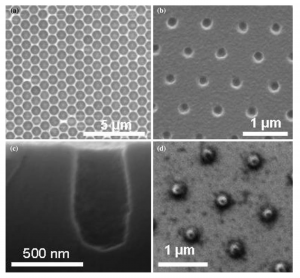 |
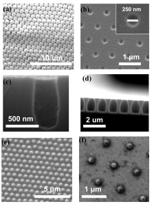
A novel self-aligned and masKless process for formation of highly uniform arrays of nanoholes and nano pillarsW. Wu, D. Dey, O. G. Memis, A. Katsnelson and H. Mohseni Nanoscale Research Letters (2007) |
 |
A deep sub-wavelength process for the formation of highly uniform arrays of nanoholes and nano pillarsW. Wu, A. Katsnelson, O. G. Memis and H. Mohseni Nanotechnology (2007) |
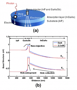 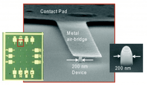 |
A photon detector with very high gain at low bias and at room temperatureO. G. Memis, A. Katsnelson, S. Kong, H. Mohseni, M. Yan, S. Zhang, T. Hossain, N. Jin and I. Adesida Applied Physics Letters (2007) |